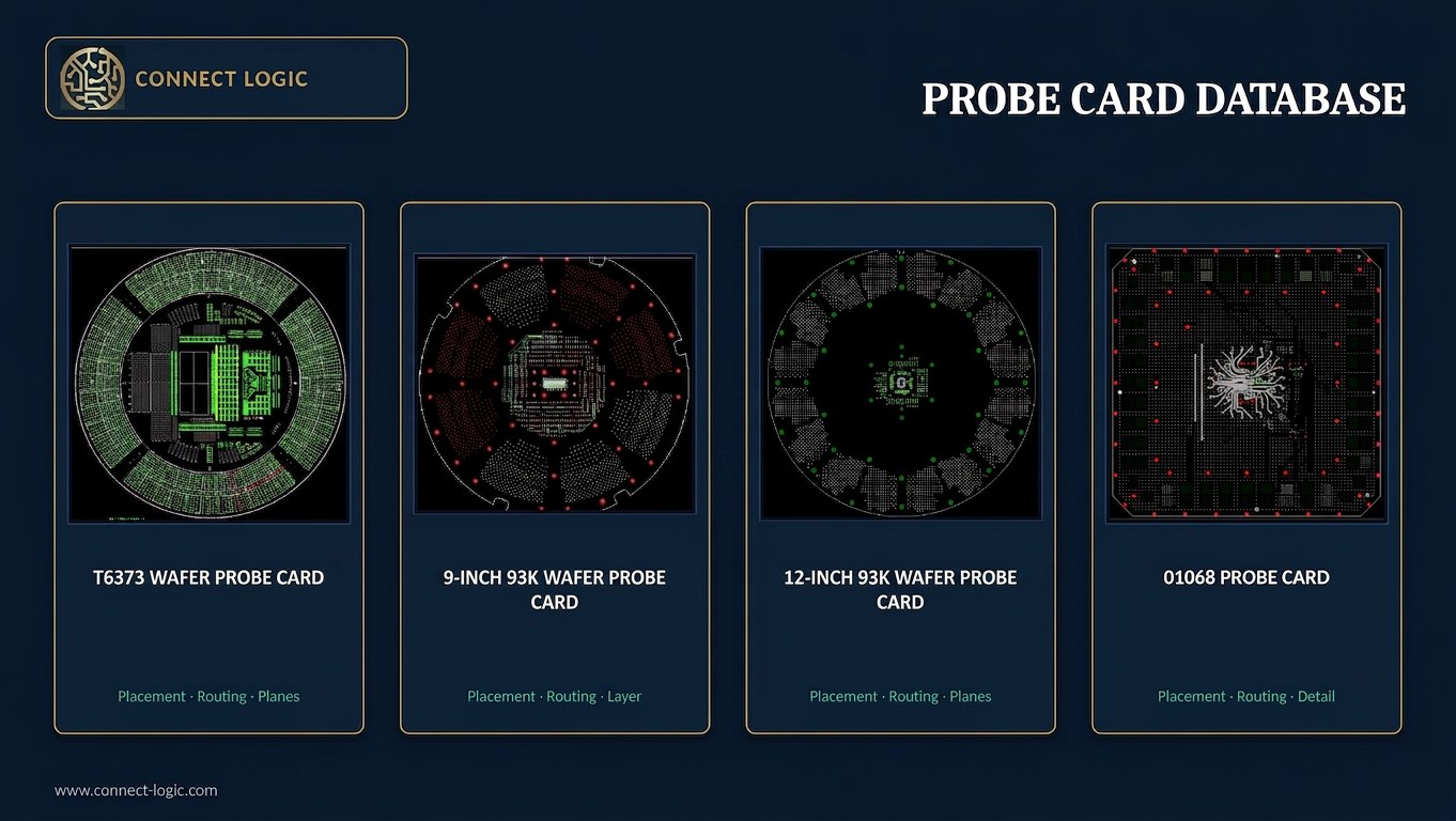
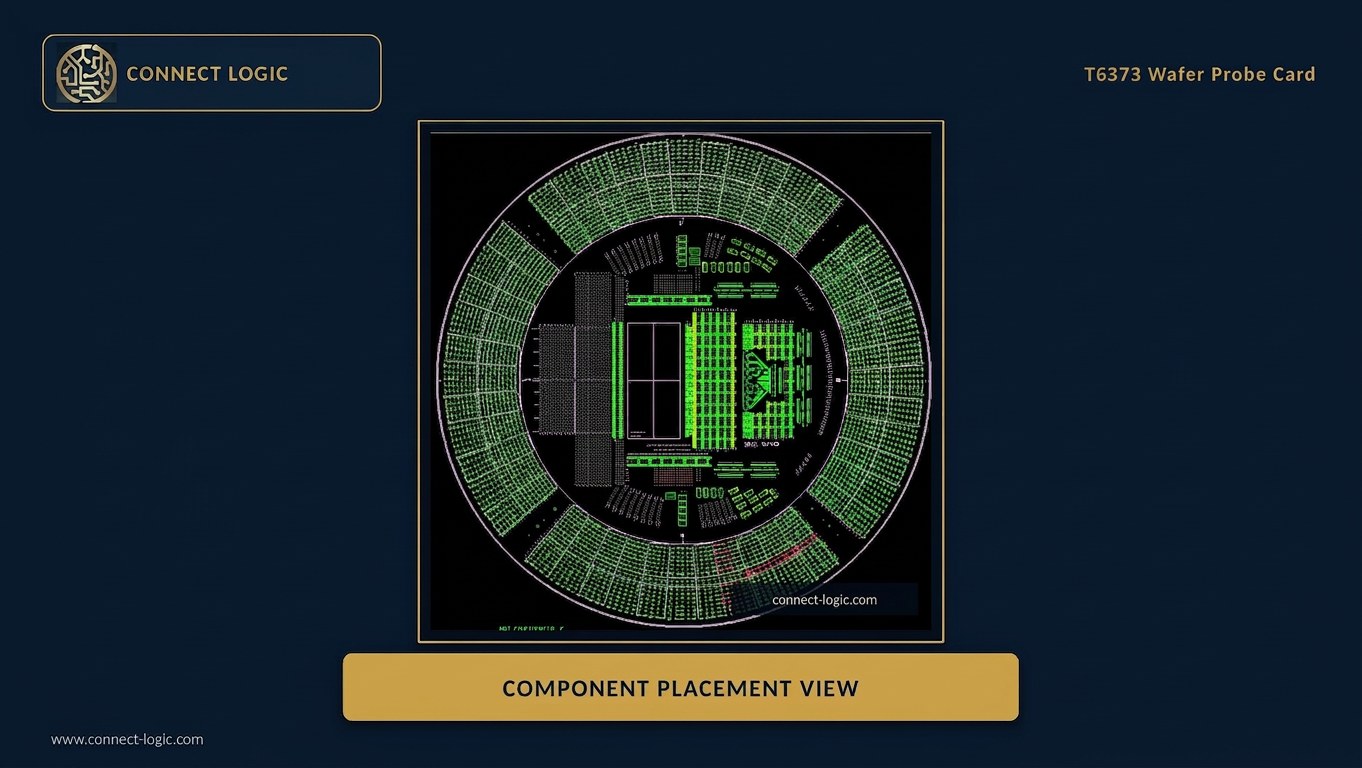
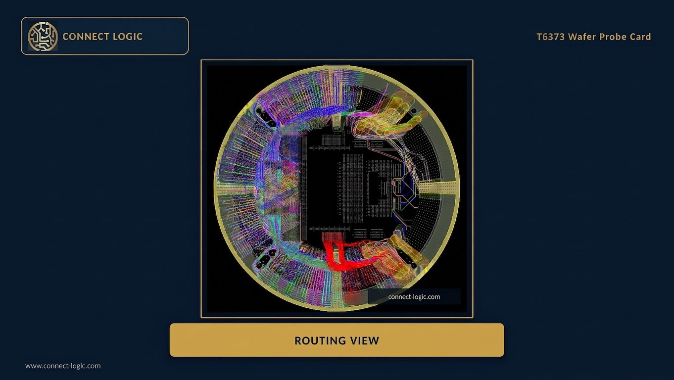
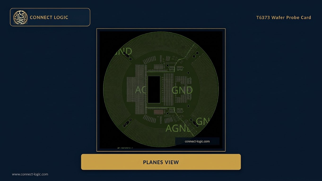
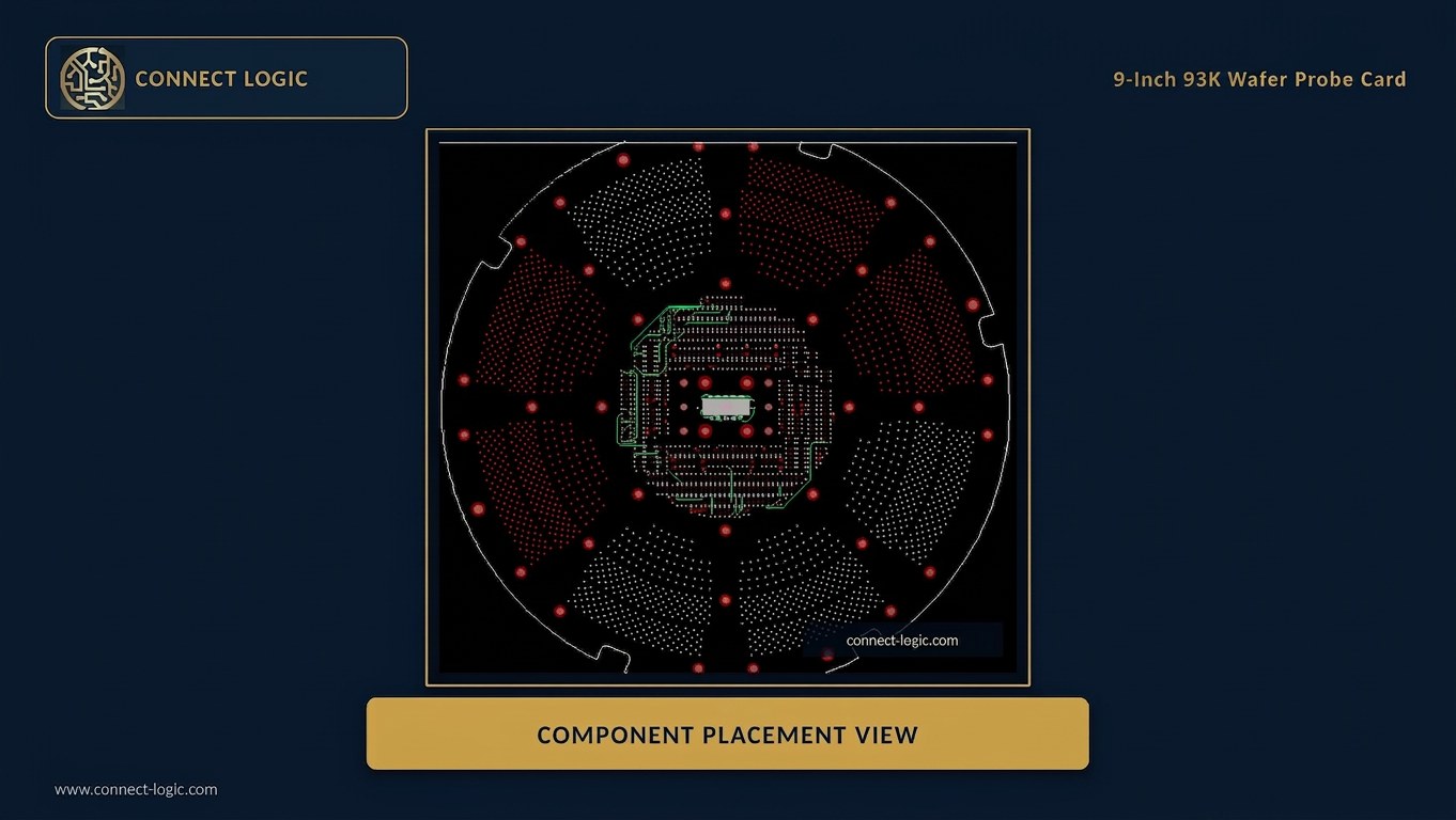
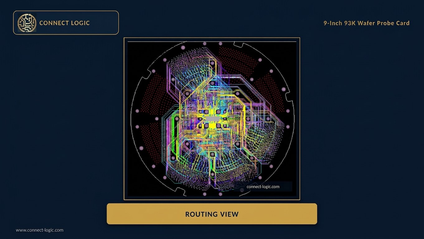
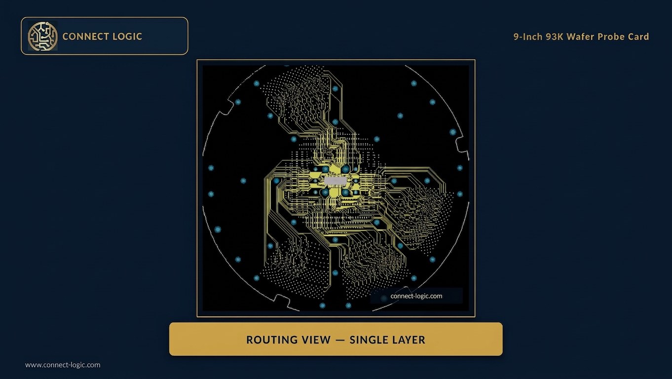
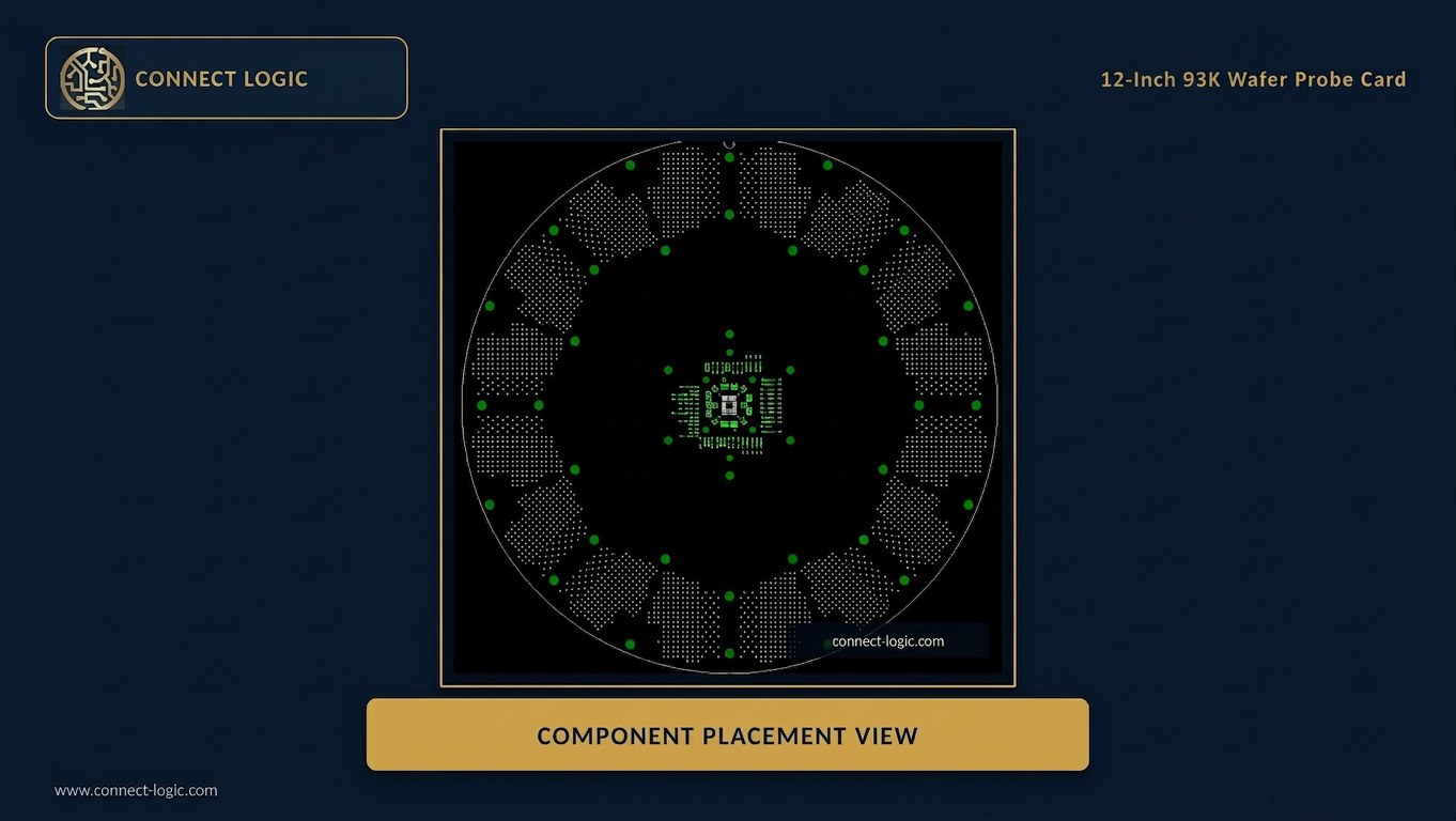
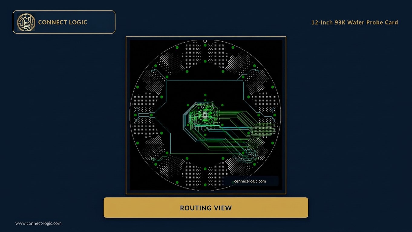
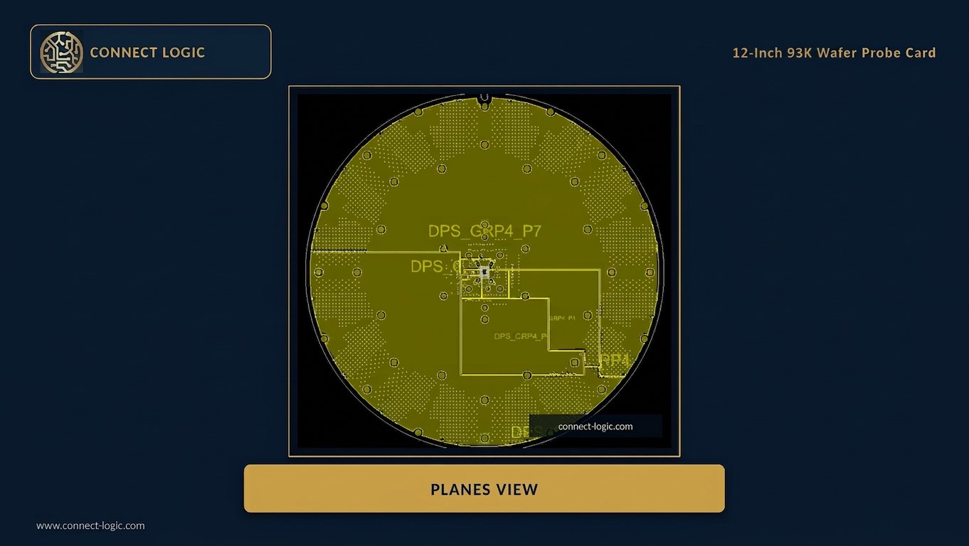
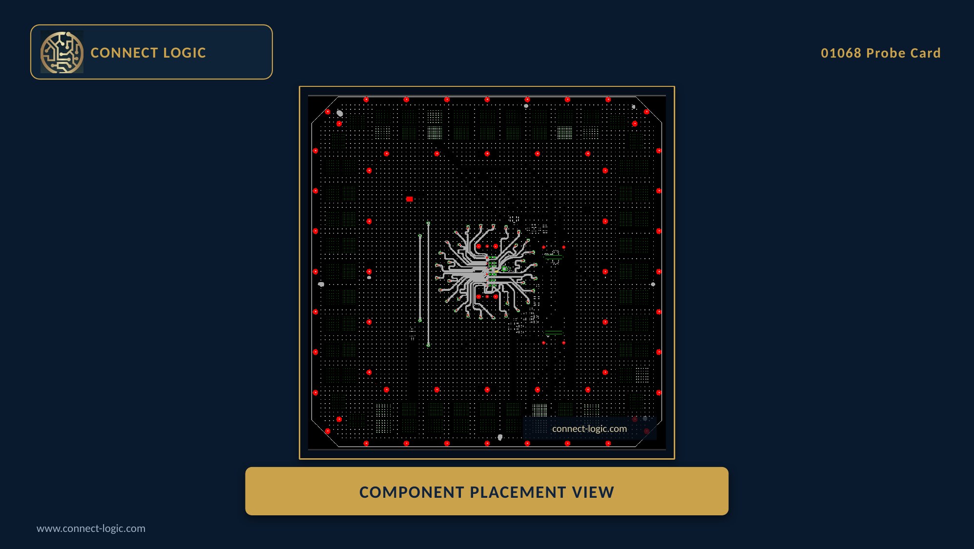
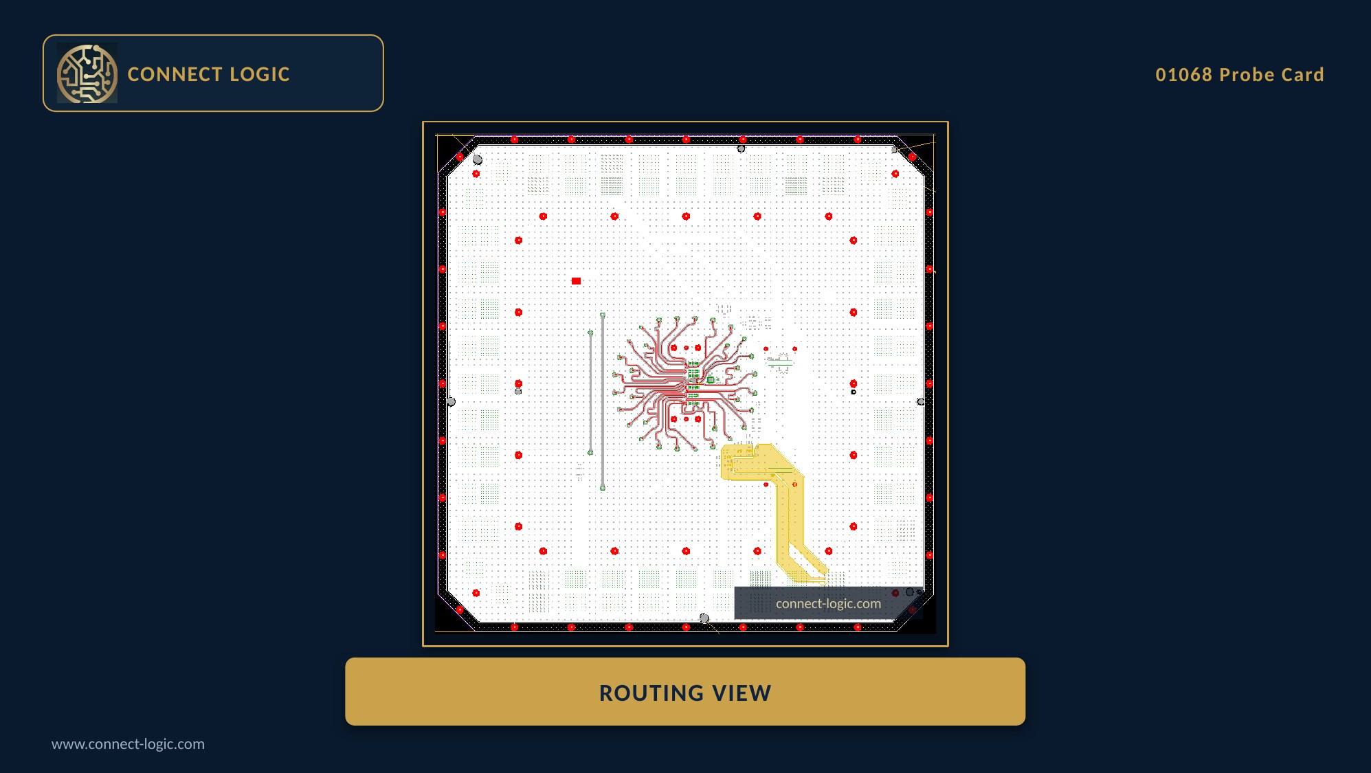
Probe Card Layout
Vertical, cantilever & MEMS. Wafer level test, perfected
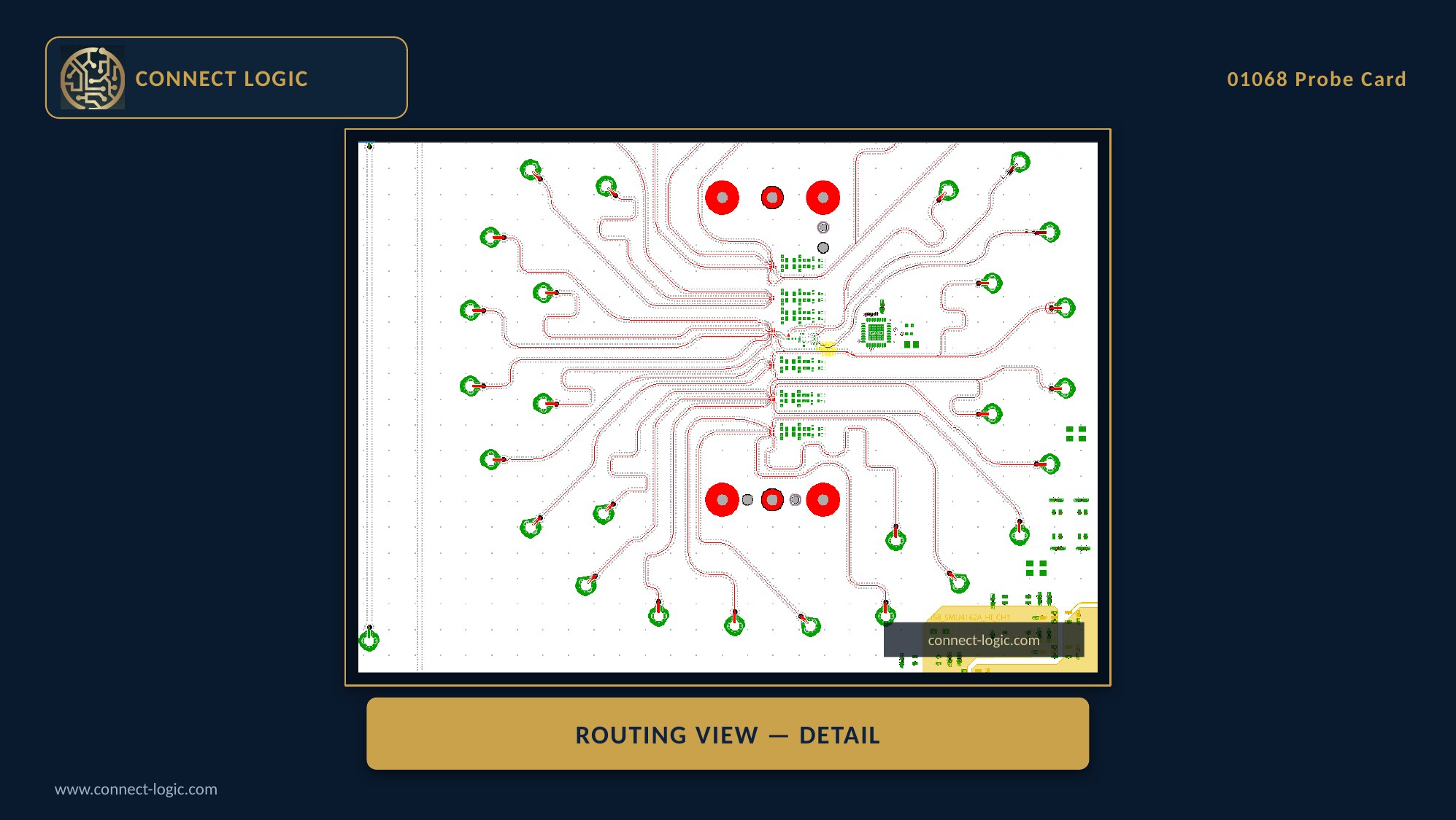
Wafer level testing is unforgiving: a small slip in controlled impedance or a few mils of DQ/DQS skew can close the eye, trigger false fails, and force costly reprobes. Our probe card design services start with pre layout SI constraints and a clean pin map / channel plan for Advantest 93K, Teradyne J750, NI STS and more. We engineer controlled impedance stackups (50 / 100 Ω), build matched length groups to ±1 mil, and use RF aware routing with stitched reference planes and back drill to minimize stubs. Validation with IBIS-AMI, TDR and S-parameters ensures stable, repeatable wafer level results. Boost yield and hit the market faster.
What we deliver in this discipline.
- Vertical, cantilever & MEMS probe cards
- Direct docking, multi site, high layer count memory
- Controlled impedance stackups (50 / 100 Ω)
- Matched length groups to ±1 mil (DQ/DQS, high speed)
- RF aware routing with stitched reference planes & back drill
- IBIS-AMI, TDR & S-parameter validation
- Platforms: Advantest 93K · Teradyne J750 · NI STS · Advantest T2000
- Up to 96 layers · 0.4 / 0.315 mm sockets · blind/buried/stacked vias
So wafer data reflects the die
Not probe card parasitics.
Problem. Late deliveries derail test schedules and time to market.
Solution. Efficient workflows and clear communication ensure layouts arrive exactly when needed.
Deliverables
- ›Layout CAD files (Allegro / Altium)
- ›Schematics + BOM
- ›Fabrication & assembly data
- ›Gerber + drill + ODB++
- ›Length & impedance reports
- ›SI validation (IBIS-AMI, TDR, S-parameters)
Save50% OFF
Your First PCB Design Project
New clients only. Kick off your first load board, probe card, or SI/PI simulation engagement at half the standard rate. Precision engineering, exceptional value.
Offer applies to first time engagements · NDA included · No obligation quote
Up to 96 layers · Blind/buried + back drill · Matched length ±1 mil · Case examples: 93K direct docking (20k pins) · J750 EX cantilever (663 signals)
Probe Card FAQs
Vertical, cantilever and MEMS. Including direct docking, multi site, and high layer count memory probe cards.
Yes. 50 / 100 Ω targets and matched length groups to ±1 mil for DQ/DQS and high speed lines.
Clean return paths, back drilled stubs, and tester aware pin maps verified with IBIS-AMI, TDR and S-parameters.
Advantest 93K, Teradyne J750, NI STS, Advantest T2000 and more.
Yes. Up to 96 layers, 0.4 / 0.315 mm sockets, blind/buried/stacked vias.
Yes. RF aware routing and S-parameter checks for loss / return loss.
About 1–3 weeks depending on complexity and reviews.
Absolutely. We work under your NDA and keep data protected.