High performance PCB layouts, engineered for semiconductor testing.
25 years of expertise crafting load boards, probe cards, and burn in boards. Backed by full signal integrity and power integrity simulation.
Simulation validated engineering, by the numbers.
Six disciplines. One uncompromising engineering standard.
Load Boards
The mechanical and electrical interface between the Device Under Test and Automatic Test Equipment. Engineered for repeatable, low noise production testing.
- Advantest 93K Full Size
- Teradyne UltraFlex / UltraFlex Plus
- Teradyne J750 · Catalyst
- Credence D-10 and more
Probe Card Layout
Vertical, cantilever and MEMS probe card layouts. Impedance control, delay matching, and RF aware routing for accurate wafer level test.
- Vertical, cantilever & MEMS probe cards
- Direct docking, multi site, high layer count memory
- Controlled impedance stackups (50 / 100 Ω)
- Matched length groups to ±1 mil (DQ/DQS, high speed)
- RF aware routing with stitched reference planes & back drill
- IBIS-AMI, TDR & S-parameter validation
- Platforms: Advantest 93K · Teradyne J750 · NI STS · Advantest T2000
- Up to 96 layers · 0.4 / 0.315 mm sockets · blind/buried/stacked vias
Burn in Boards
Burn in boards that stress ICs under controlled conditions to expose early life failures. Engineered for thermal endurance and consistent results.
- HPB3/5 BIB · HPB 4
- HAST THB-85/85
- High temperature stackups
- High pin count fixtures
Signal Integrity (SI)
Full SI simulation and validation. Via impedance optimization, S-parameter extraction, TDR plots, eye diagrams, crosstalk, EMI/EMC compliance, and failure root cause analysis.
- Via impedance optimization
- S-Parameter extraction
- TDR impedance plot
- Time domain analysis (eye, IBIS-AMI, skew, compliance)
- RF channel analysis
- Crosstalk analysis
- RLGC extraction & EMI
- EMI / EMC failure board analysis
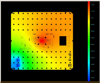
Power Integrity & Thermal
DC IR drop, Z11 impedance, decap optimization, SSN/SSO, and electrical thermal co simulation for power dense modern silicon.
- DC IR drop · Power impedance Z11
- Decap optimization
- SSN/SSO analysis
- Thermal & electrical thermal co sim
MLO Package Design
Multi layer organic substrate and package layout with full simulation. Flagship reference: 4,714 die pins, 556 signals at 1500 MHz, ~1 month including review.
- Bump pitch from 150 µm
- BGA arrays to 49×49 @ 1000 µm
- Stackups incl. 5-2-5 (BU-C-BU)
- Layout, length & pin reports
HDI-RF & Commercial PCB Design
HDI + RF/microwave PCB layout with controlled-impedance stackups, microvias, back-drill, hybrid stripline/microstrip mixes, and EMI/EMC-aware routing for clean eyes and quiet emissions.
- Interfaces: DDR2/3/4, USB, PCIe, SATA, HDMI, LVDS, MIPI, SERDES to 112 Gbps
- HDI: microvia stacks (1–3), blind/buried/stacked, 0.4 / 0.315 mm BGA, 0.1 mm microvia drills
- Hybrid stackups: stripline & microstrip mixes; thickness 0.92–6.35 mm
- Impedance control ±5% (50 / 90 / 100 Ω); multi-impedance on the same layer
- Length-matched groups, phase tuning, arc routing for RF
- Return-path integrity: stitching, back-drill, blind/buried stub removal
- PDN/decoupling optimized by frequency · low-Z rails (Z11)
- EMI/EMC: shielding, clean references, NEXT/FEXT crosstalk control
- Layer counts: 6–48 typical for HDI
Two ways a test program can go.
Noise. Respins. Missed dates.
- Inaccurate, unrepeatable test results
- Costly board respins from undetected SI/PI issues
- Missed deadlines that derail test schedules
- High frequency designs failing at the limit
Minimized noise. Maximum integrity.
- Reliable, repeatable testing by design
- Simulation validated layouts; fewer respins
- On time delivery with clear communication
- Engineered up to 50 GHz and 1000 A
The pain points engineers bring us, and how we solve them.
Noisy boards and poor signal integrity yield inaccurate, unrepeatable test results.
Meticulous, simulation validated layouts that minimize noise and maximize signal integrity for reliable, repeatable testing.
Late deliveries derail test schedules and time to market.
Efficient workflows and clear communication ensure layouts arrive exactly when needed.
Costly board respins from undetected SI/PI issues.
Full SI/PI simulation, eye diagrams, TDR, IR drop, decap optimization, validates designs before fabrication.
High frequency, high current designs failing at the limit.
Boards engineered up to 50 GHz and 1000 A with controlled impedance (±5%) and matched length (±1 mil).
Premium design quality assumed to be unaffordable.
Competitive rates without compromising performance or service. 25 years of disciplined engineering.
Four goals that govern every design we deliver.
High Quality
Engineered for excellence. Meticulous design and premium practices minimize noise and maximize signal integrity for reliable, repeatable testing.
On Time Delivery
Efficient workflows and clear communication mean layouts arrive exactly when needed.
Affordable Rates
Competitive pricing without sacrificing performance or service.
Customer Satisfaction
Outstanding high frequency performance you can trust. Partnerships, not transactions.
High density MLO package design.
Routing LVDS between two dies was critical; achieved IL, RL and PDN targets. 0402 decoupling caps added die side for critical power. Delivered including simulation, review and approval.
Read the full case| Die pin count | 4,714 |
| Die size | 30 × 17.1 mm |
| Bump pitch | 150 µm |
| Package size | 50,000 × 50,000 µm |
| BGA array | 49 × 49 @ 1000 µm pitch |
| Package thickness | 890 µm |
| Signals | 556 incl. DDR4 & LVDS @ 1500 MHz |
| Stackup | 5-2-5 (BU-C-BU) |
| Lead time | ~1 month (incl. sim, review, approval) |
Partner with us and unlock the full potential of your ATE platform.
Contact us today for a free consultation and discover how our PCB layout designs can revolutionize your testing process.