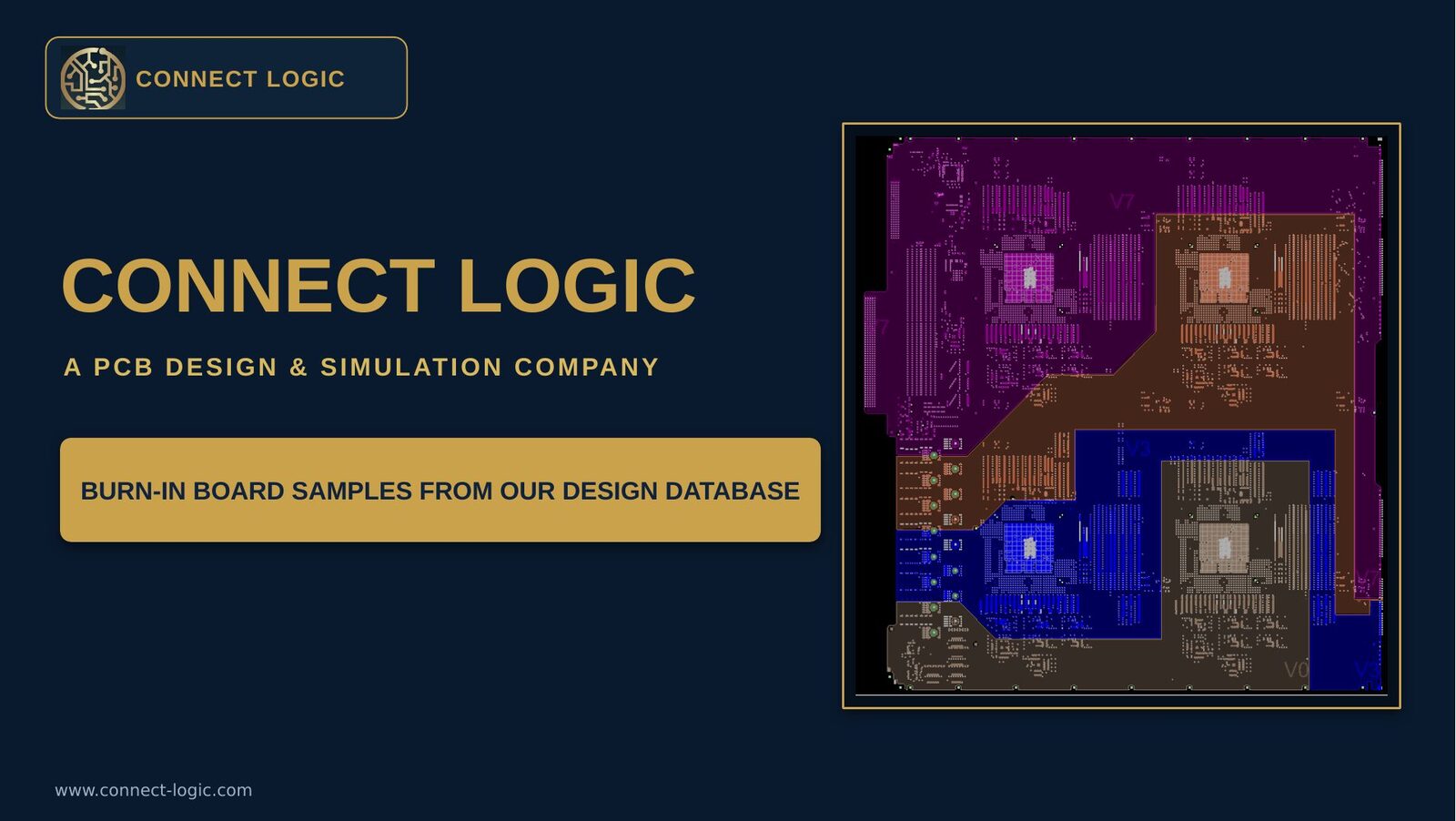
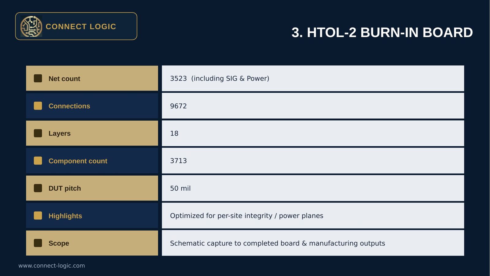
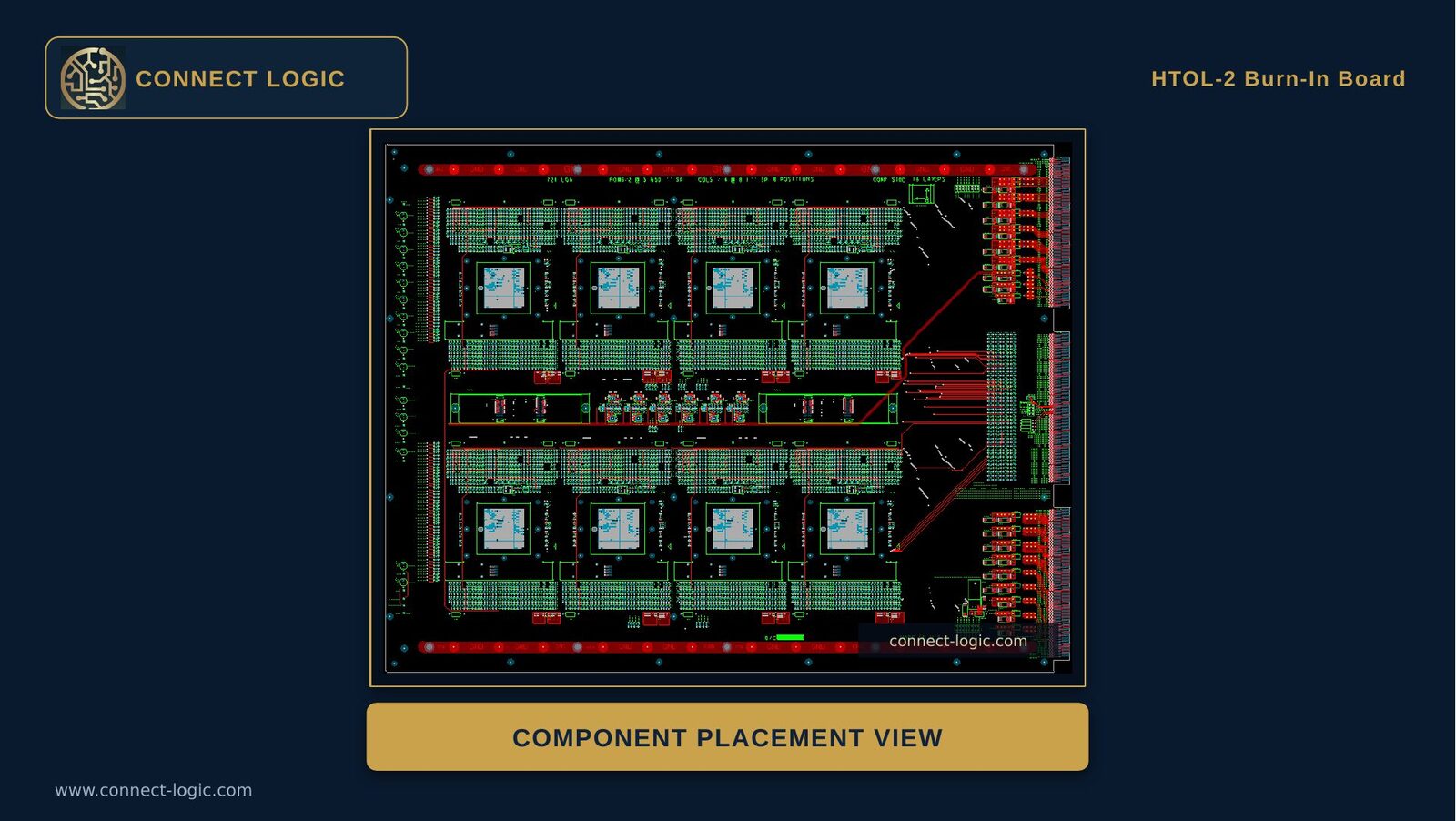
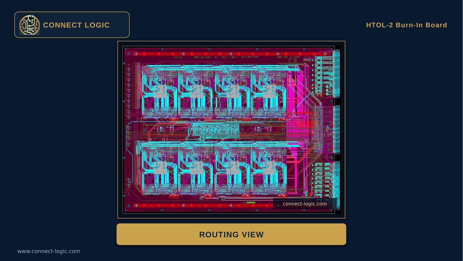
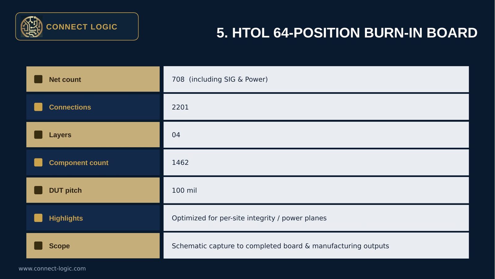
Burn in Boards
Reliability stress testing, designed for endurance
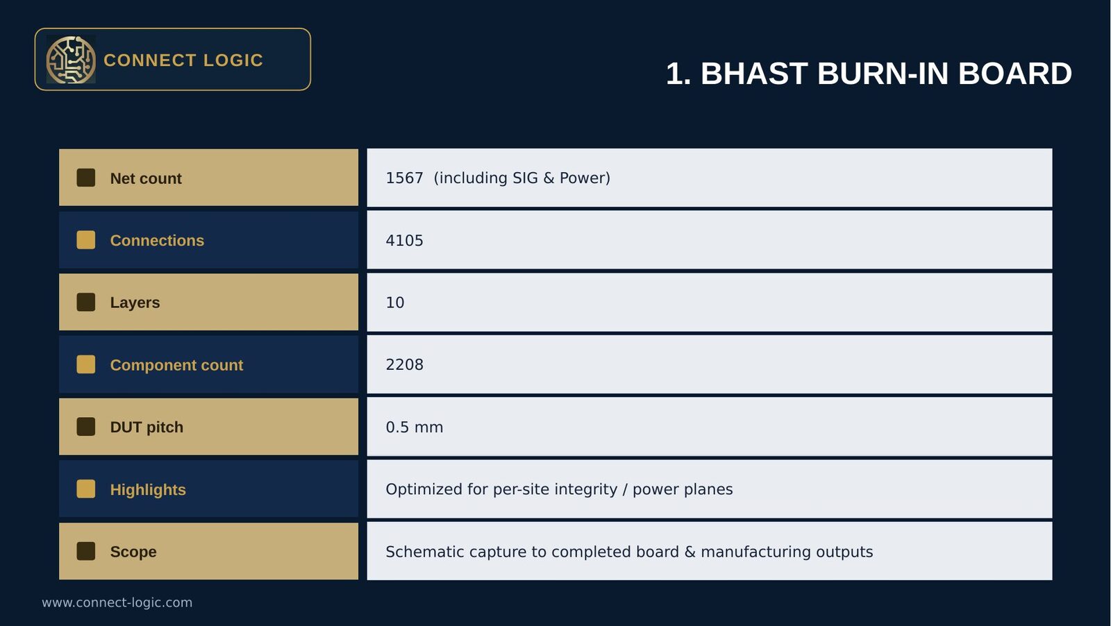
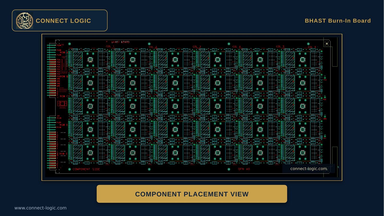
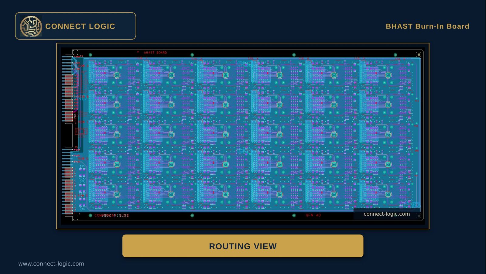
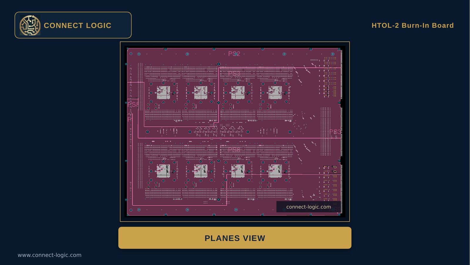
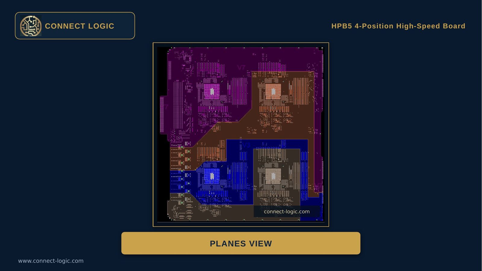
High volume burn in is unforgiving. Hotspots, uneven airflow, or marginal copper can trigger thermal runaway, early fails, and costly retests, and long soak times at elevated voltage and high current expose any weakness in power delivery, skewing your stress data and stretching schedules. We design BIBs for HPB5/HPB4 systems with low impedance power planes (wide copper, via stitching), thermal relief patterns, and well placed sensors, then verify with thermal simulation/CFD to hold junction and board temperatures in spec. Clearances and creepage are tuned for higher voltages, and traces are derated for high current, so your burn in results reflect the device's behavior, not the board's limits.
What we deliver in this discipline.
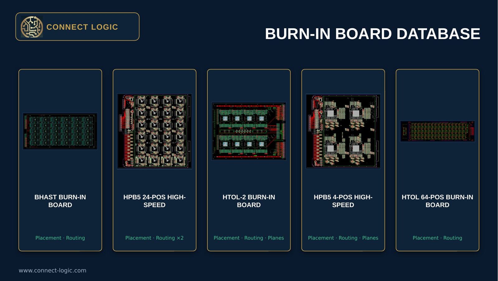
- HPB3/5 BIB · HPB 4
- HAST THB-85/85
- High temperature stackups
- High pin count fixtures
Hotspots, uneven airflow, or marginal copper can trigger thermal runaway and costly retests. Long soak times at elevated voltage and high current expose any weakness in power delivery, skewing stress data and stretching schedules. We design BIBs with low impedance power planes, thermal relief patterns, and well placed sensors, then verify with thermal simulation/CFD to hold junction and board temperatures in spec.
So burn in results reflect device behavior
Not board limits.
Problem. High frequency, high current designs failing at the limit.
Solution. Boards engineered up to 50 GHz and 1000 A with controlled impedance (±5%) and matched length (±1 mil).
Deliverables
- ›Thermally aware layout
- ›Schematics + BOM
- ›Fabrication & assembly pack
Save50% OFF
Your First PCB Design Project
New clients only. Kick off your first load board, probe card, or SI/PI simulation engagement at half the standard rate. Precision engineering, exceptional value.
Offer applies to first time engagements · NDA included · No obligation quote
HPB3/5 BIB · HPB 4 · HAST THB-85/85 · Thermal simulation/CFD · High-Tg laminates · Wide copper · Via stitching · Creepage & clearance
Burn-in Board FAQs
A PCB that stresses devices under HTOL/HAST to screen early failures, often on HPB5/HPB4 systems.
Yes, wide copper, via stitching, and creepage/clearance rules; traces derated for current.
Thermal simulation/CFD, copper balancing, thermal reliefs, and sensor placement to keep temps in spec.
High-Tg laminates and thicker copper options per reliability/DFM needs.
Stackup, Gerbers/ODB++, drill, fab/assembly notes, test coupons (as required).
Usually 1–3 weeks, subject to complexity and review cycles.
We serve globally, primarily the USA, plus Canada, Europe, Singapore, Malaysia, Taiwan, Germany, and Japan.
Absolutely, we work under your NDA and keep data protected.