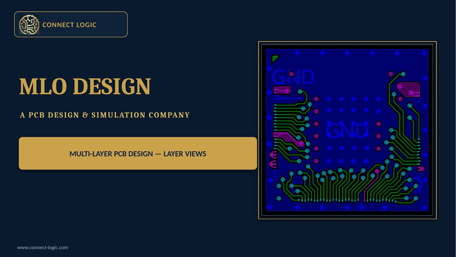
MLO Package Design
High density organic substrate layout
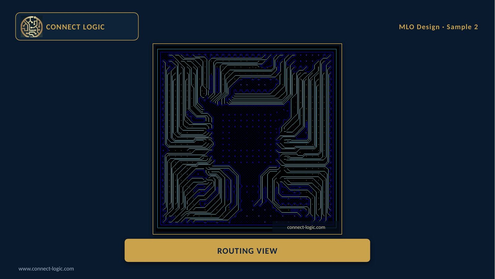
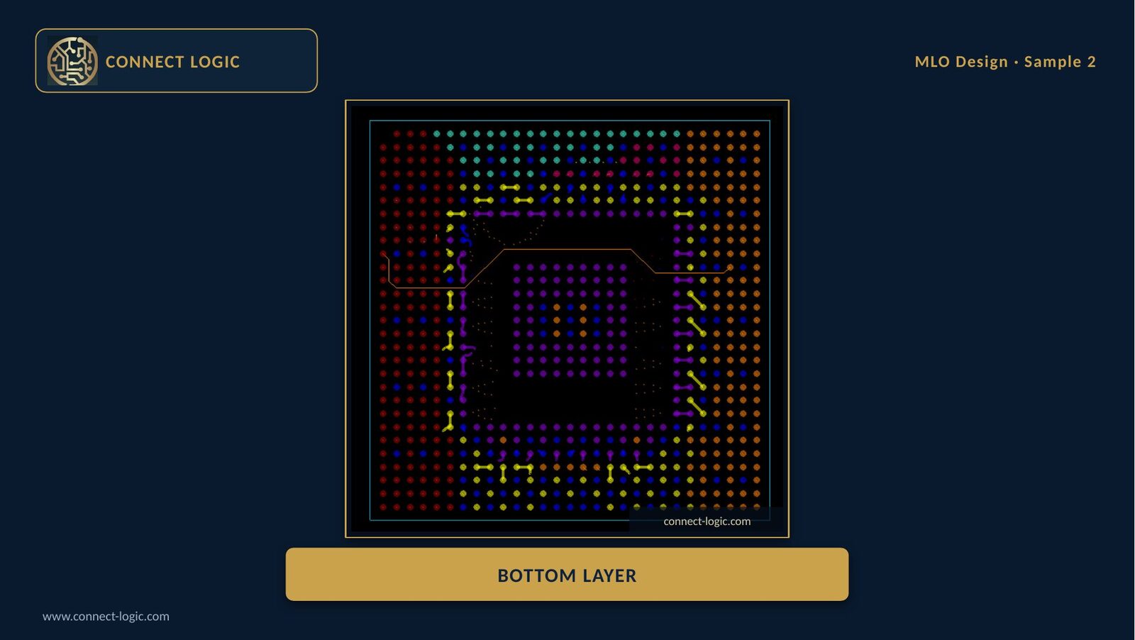
Multi layer organic substrate / package layout and simulation. Flagship reference: 4,714 die pins, 556 signals at 1500 MHz, 49×49 BGA at 1000 µm pitch, delivered in ~1 month including simulation, review and approval.
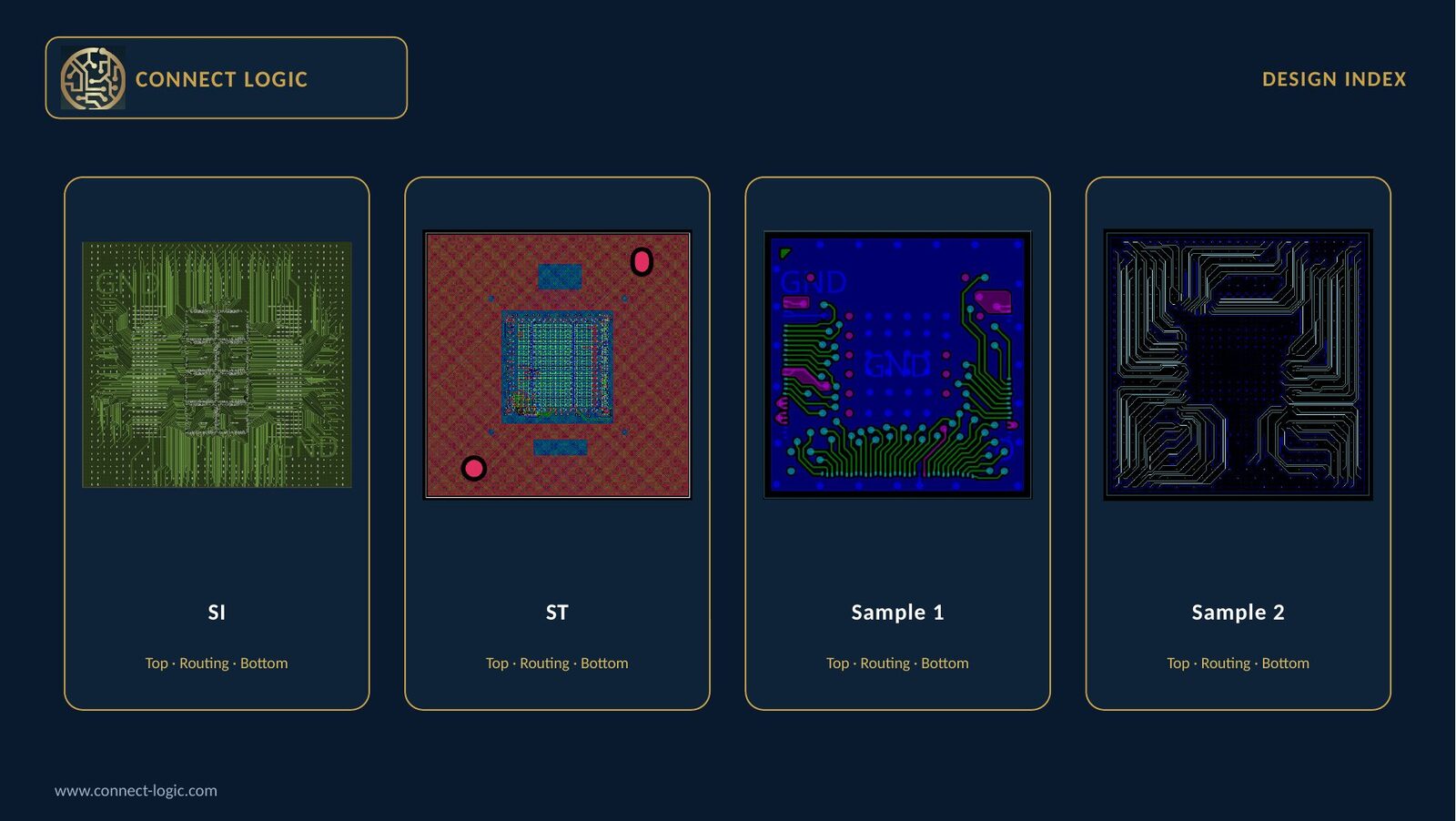

What we deliver in this discipline.
- Bump pitch from 150 µm
- BGA arrays to 49×49 @ 1000 µm
- Stackups incl. 5-2-5 (BU-C-BU)
- Layout, length & pin reports
Problem. Noisy boards and poor signal integrity yield inaccurate, unrepeatable test results.
Solution. Meticulous, simulation validated layouts that minimize noise and maximize signal integrity for reliable, repeatable testing.
Deliverables
- ›Layout in .mcm / .brd
- ›Length report
- ›Symbol pin report
- ›Gerbers + drill
- ›ODB++ (if needed)
- ›DXF + PDF layer outputs
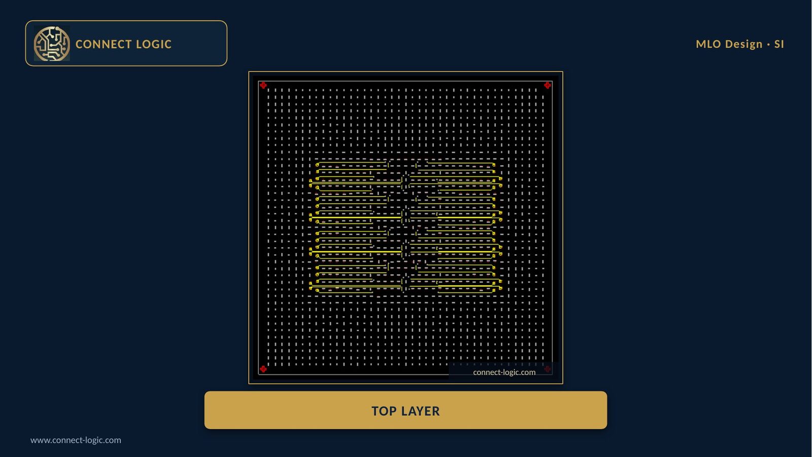
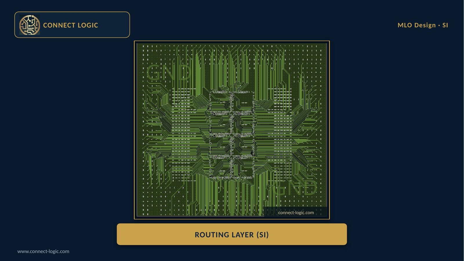
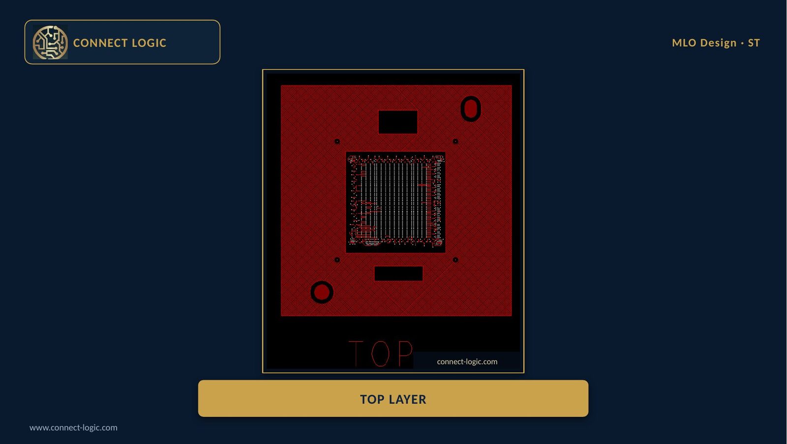
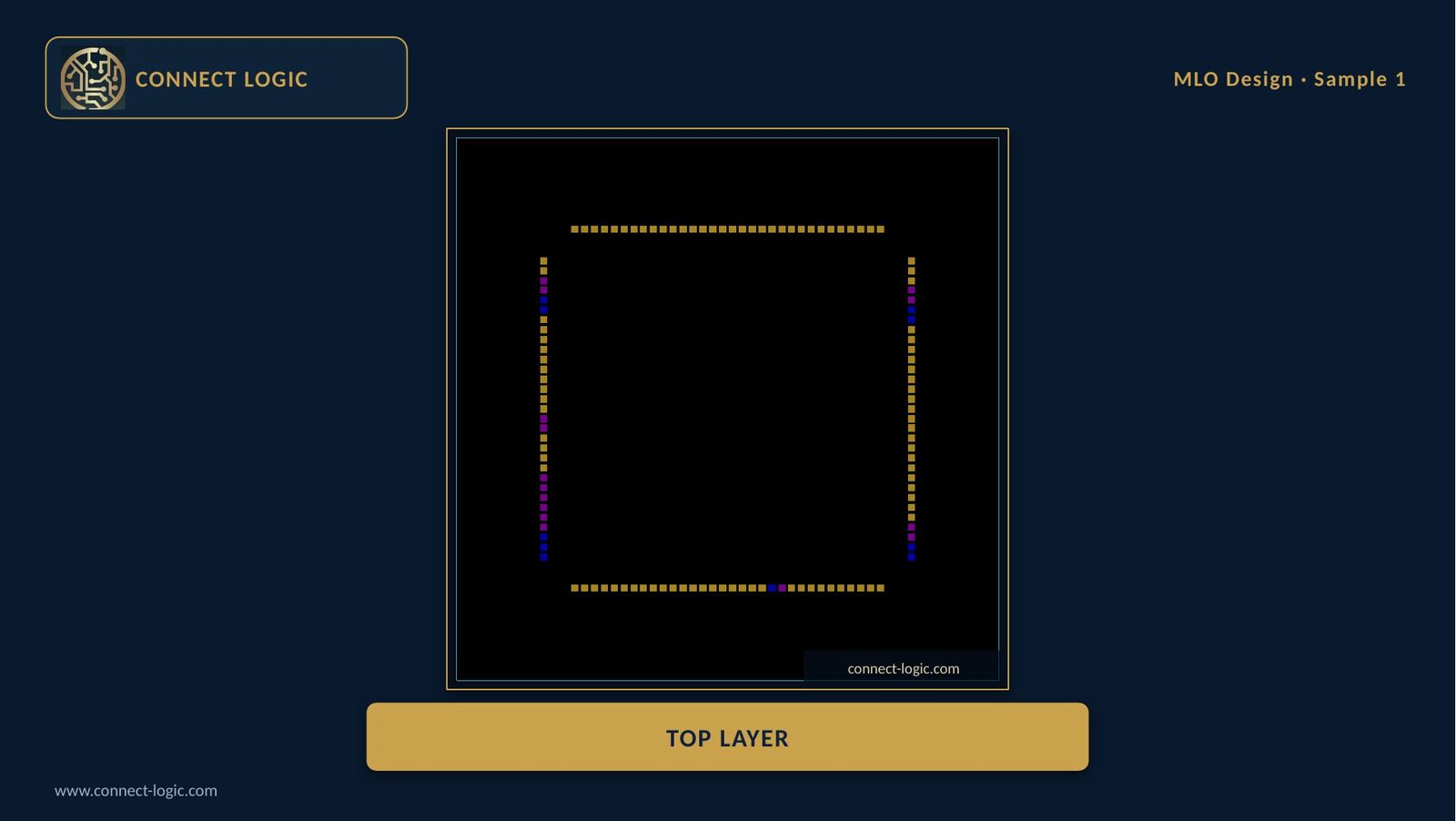
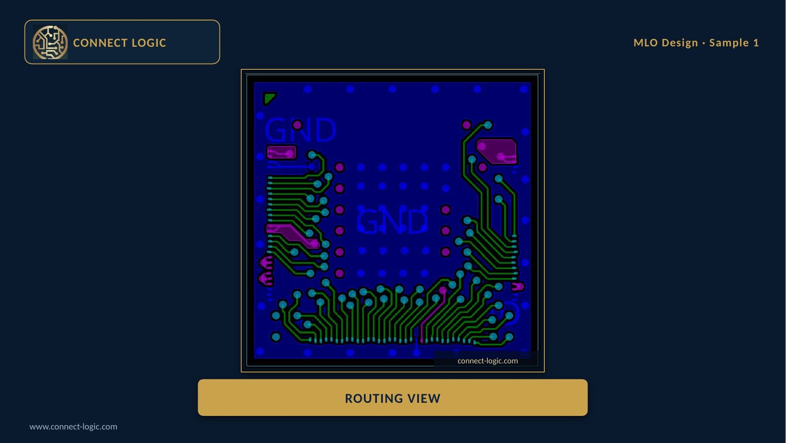
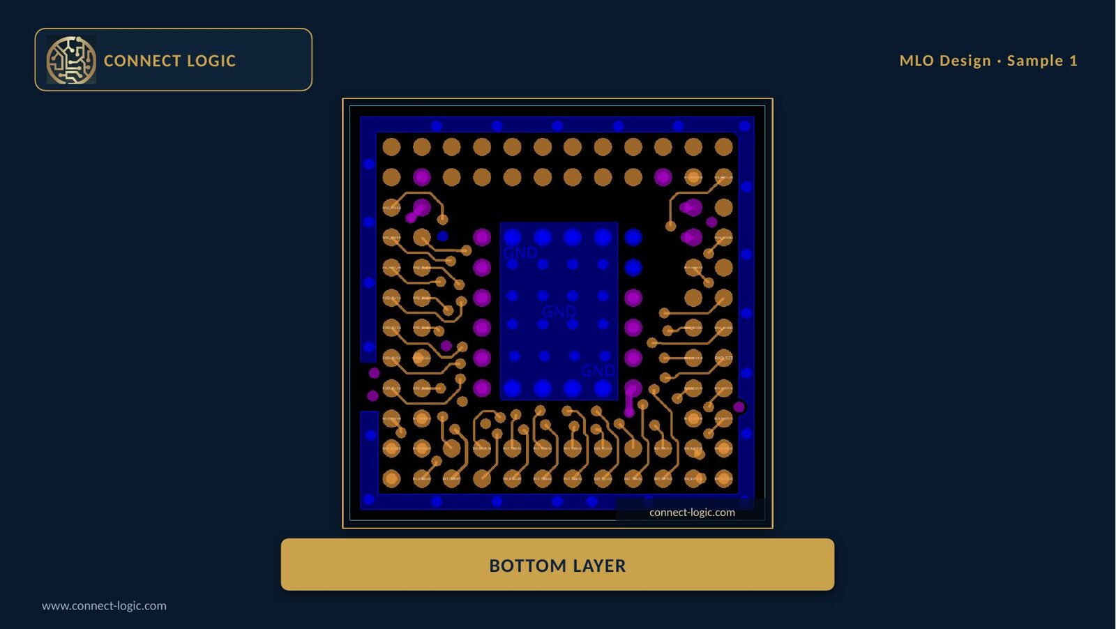
Engineering snapshot of the flagship MLO package.
4,714 die pins · 49×49 BGA · 1000 µm pitch
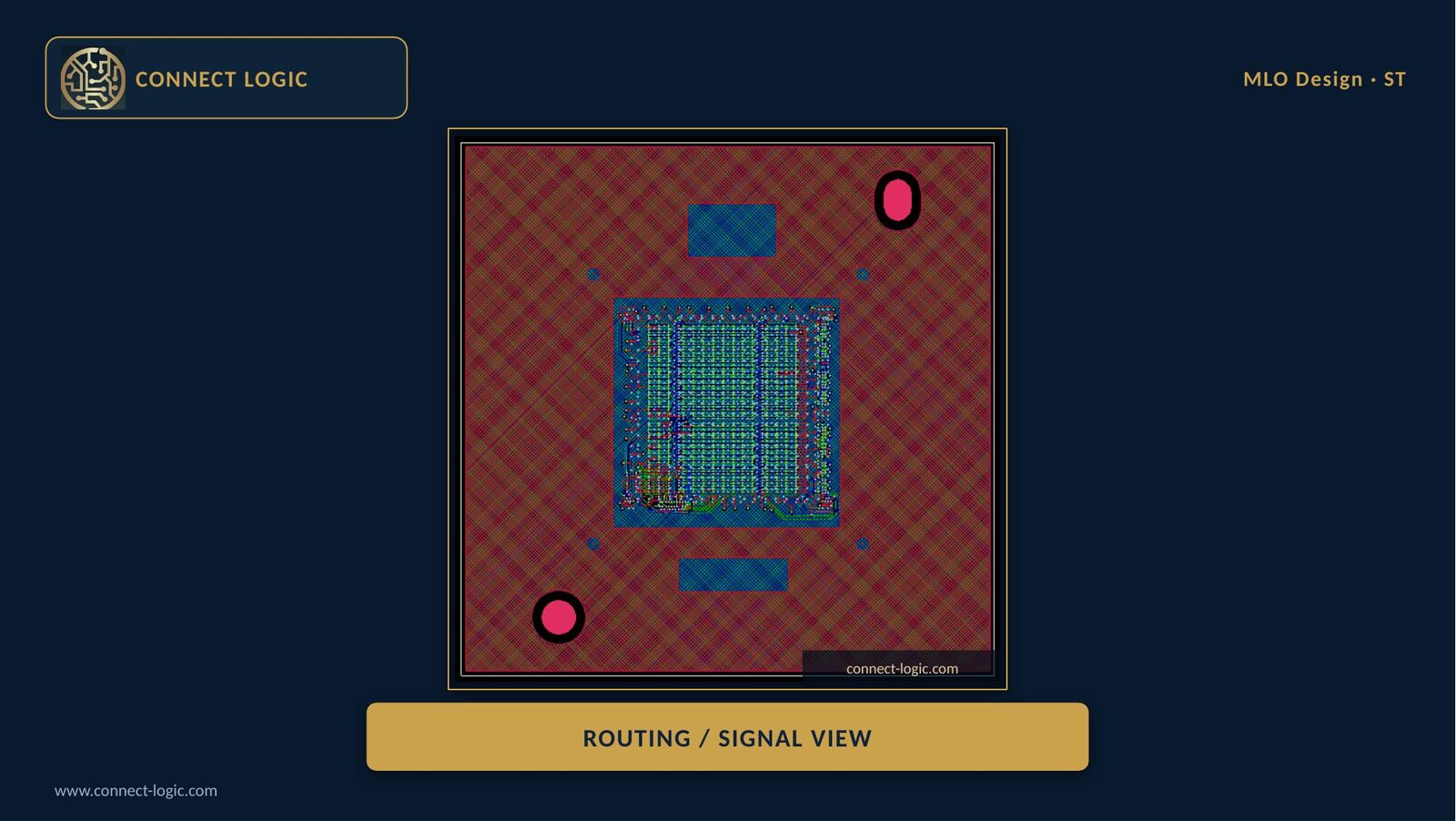
556 signals with mixed interfaces including DDR4 and LVDS running at 1500 MHz.
Routing LVDS traces between two dies is critical — achieving IL, RL and PDN targets to specification.
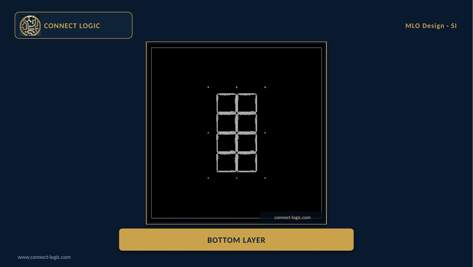
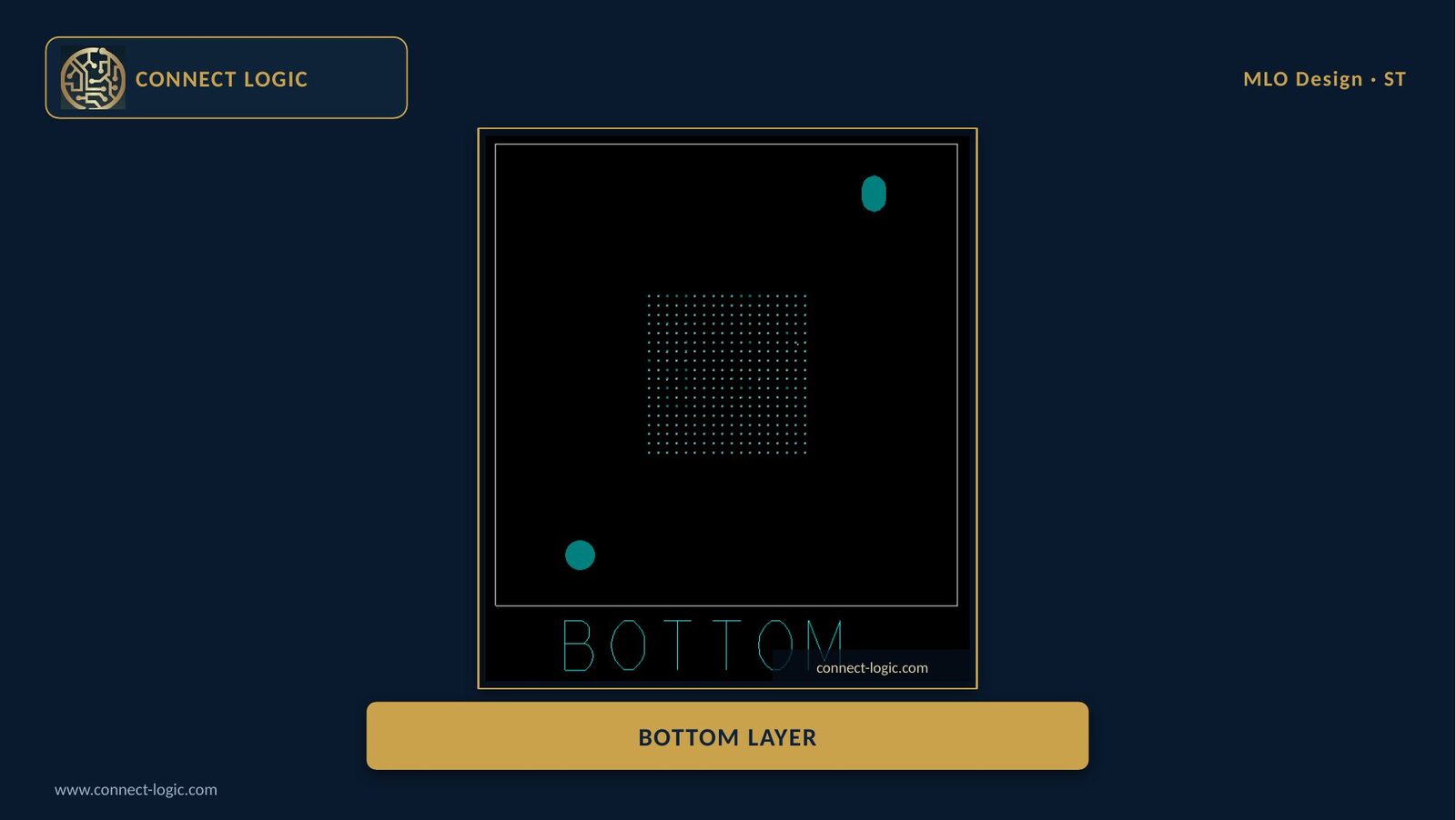
0402 package decoupling capacitors placed on the die side for critical power rails.
5-2-5 structure (BU-C-BU) — build-up / core / build-up.
~1 month including simulation, customer review and approval.