HDI-RF & Commercial PCB Design
HDI microvias · RF/microwave to 40 GHz · SERDES to 112 Gbps
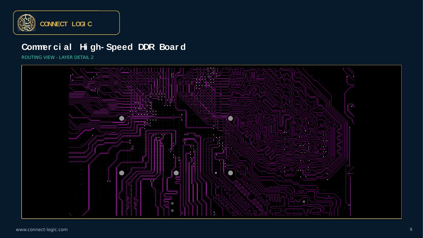
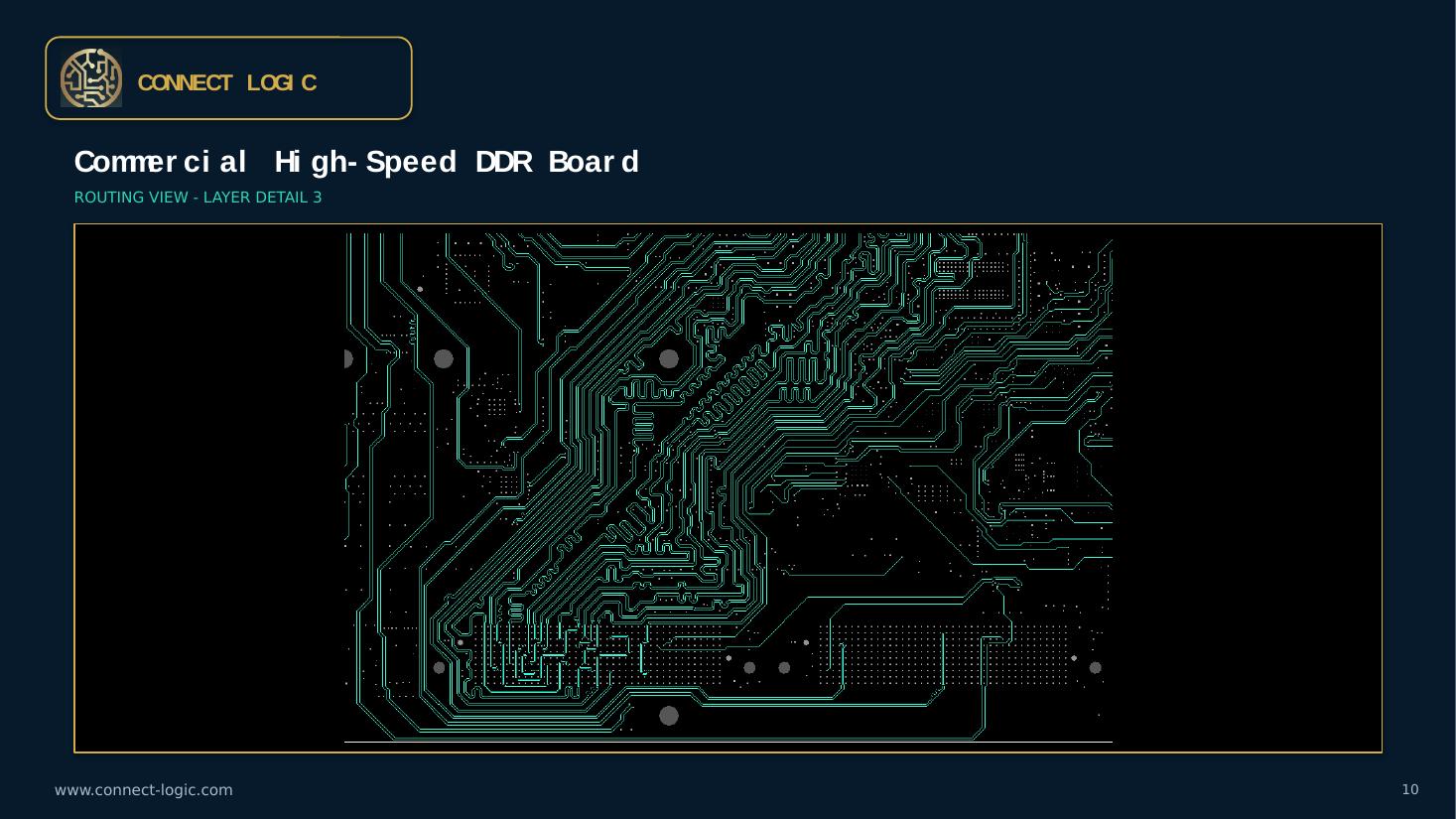
At high speeds, little things become big problems—reflections, insertion loss, mode conversion, and EMI can tank margins and spin debug loops. We design HDI + RF boards that behave: controlled-impedance stackups, stitched return paths, microvias/back-drill to kill stubs, and clean routing that keeps eyes open and emissions in check.
What we deliver in this discipline.
- Interfaces: DDR2/3/4, USB, PCIe, SATA, HDMI, LVDS, MIPI, SERDES to 112 Gbps
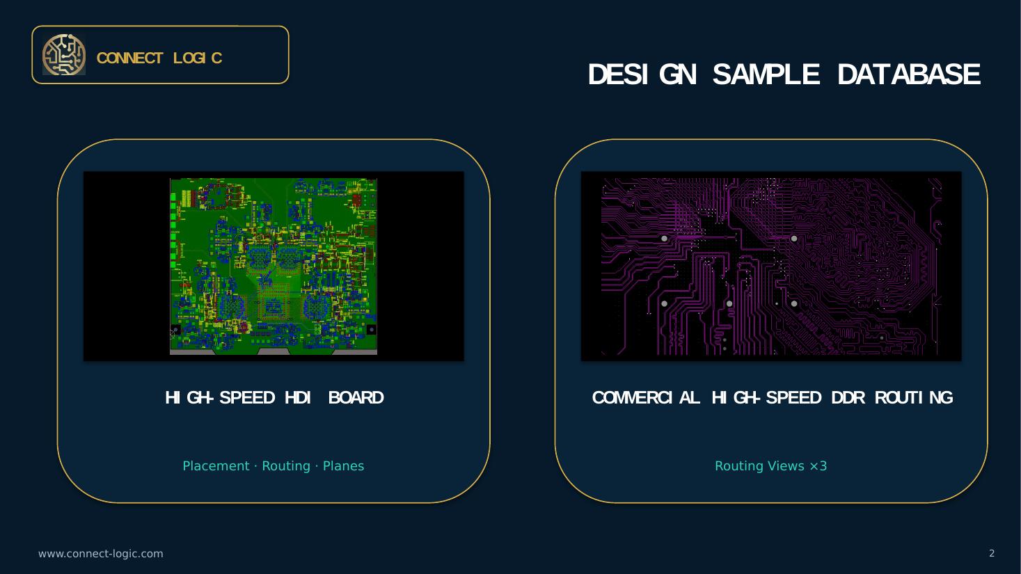
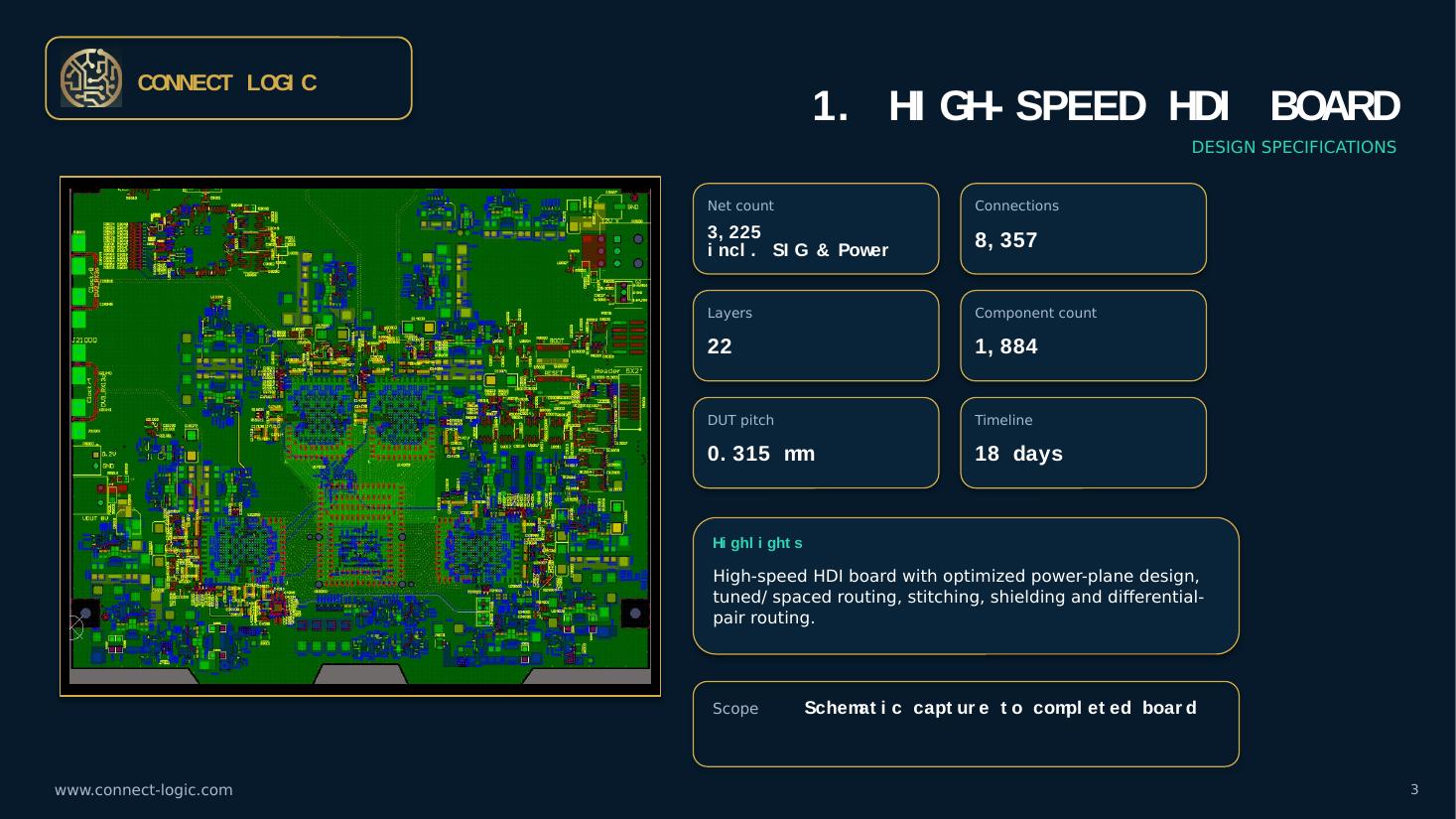
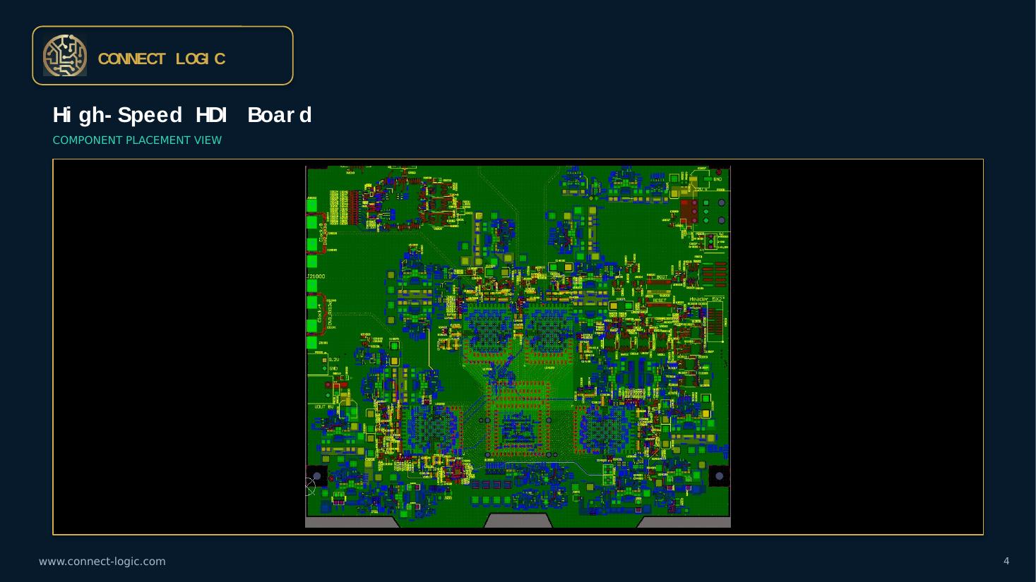
- HDI: microvia stacks (1–3), blind/buried/stacked, 0.4 / 0.315 mm BGA, 0.1 mm microvia drills
- Hybrid stackups: stripline & microstrip mixes; thickness 0.92–6.35 mm
- Impedance control ±5% (50 / 90 / 100 Ω); multi-impedance on the same layer
- Length-matched groups, phase tuning, arc routing for RF
- Return-path integrity: stitching, back-drill, blind/buried stub removal
- PDN/decoupling optimized by frequency · low-Z rails (Z11)
- EMI/EMC: shielding, clean references, NEXT/FEXT crosstalk control
- Layer counts: 6–48 typical for HDI
Problem. Late deliveries derail test schedules and time to market.
Solution. Efficient workflows and clear communication ensure layouts arrive exactly when needed.
Deliverables
- ›Stackup & constraints
- ›Gerbers / ODB++
- ›Drill files
- ›Fab & assembly notes
- ›Simulation plots (on request)
- ›Length & impedance reports
Save50% OFF
Your First PCB Design Project
New clients only. Kick off your first load board, probe card, or SI/PI simulation engagement at half the standard rate. Precision engineering, exceptional value.
Offer applies to first time engagements · NDA included · No obligation quote
Ready to discuss your hdi-rf & commercial pcb design program?
HDI microvias · RF/microwave to 40 GHz · SERDES to 112 Gbps · Controlled impedance ±5% · Hybrid stackups · Back-drill · EMI/EMC aware routing
HDI & RF FAQs
High-density interconnect using microvias, blind/buried/stacked vias, and tight rules to route fine-pitch BGAs with controlled impedance.
Yes — balanced microstrip/stripline stacks with even/odd layers, tuned for SI/PI and EMI/EMC.
Down to 0.315 / 0.4 mm BGA pitch with microvias and via-in-pad as required.
Yes, back-drill on through-hole vias or blind/buried/stacked microvias to eliminate stubs and improve IL/RL.
Layout and verification for RF/microwave to 40 GHz, with SERDES channels to 112 Gbps.
±5% impedance targets, stitched returns, spacing by frequency, and simulation of IL/RL, TDR, and crosstalk (NEXT/FEXT).
Stackup & constraints, Gerbers/ODB++, drill files, fab/assembly notes, and (if requested) simulation plots.
About 1–3 weeks, depending on complexity and review cycles.
We serve globally, primarily the USA, plus Canada, Europe, Singapore, Malaysia, Taiwan, Germany, and Japan.
Absolutely — we work under your NDA and keep data protected.